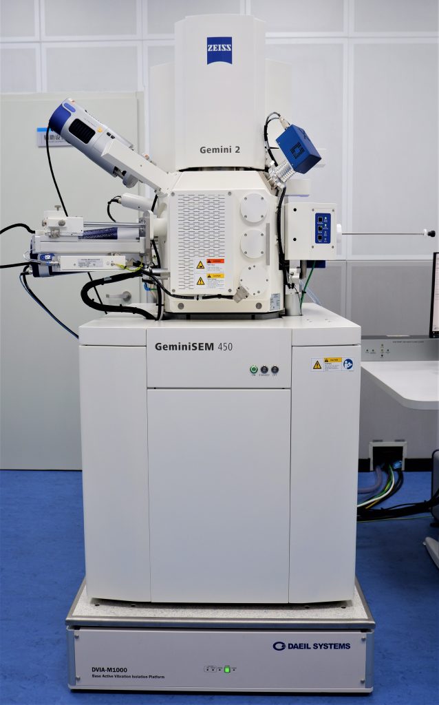
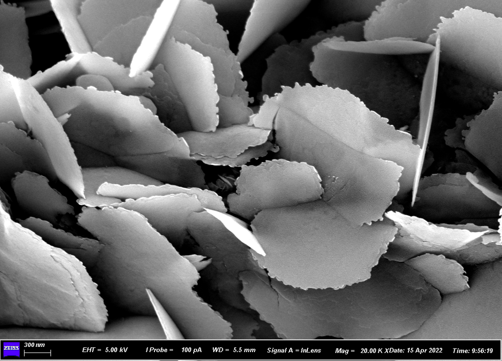
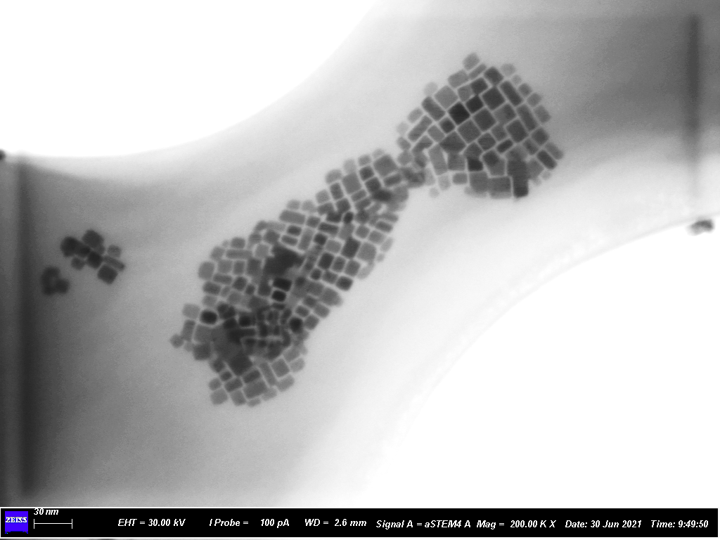
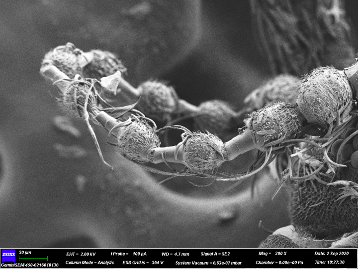
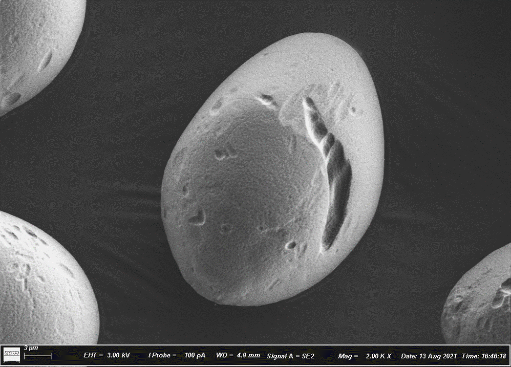
Model:
Zeiss Gemini 450
Address:
RB02
Electron optics:
Highest resolution: 0.7 nm at 15 kV
Vacuum in VP mode: 5Pa ~ 500Pa
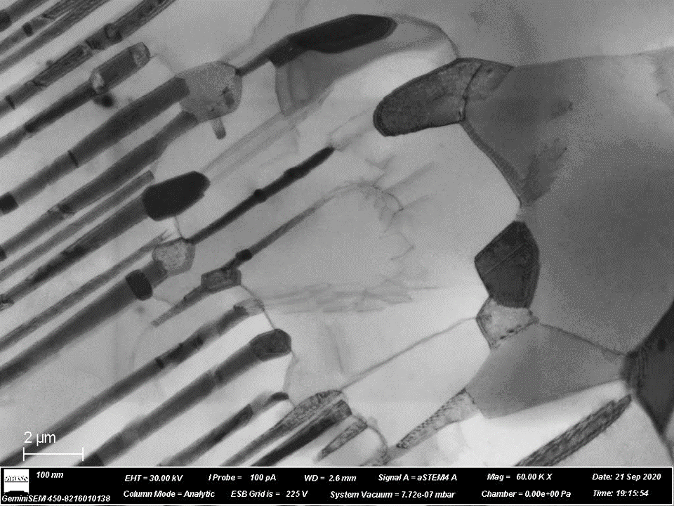
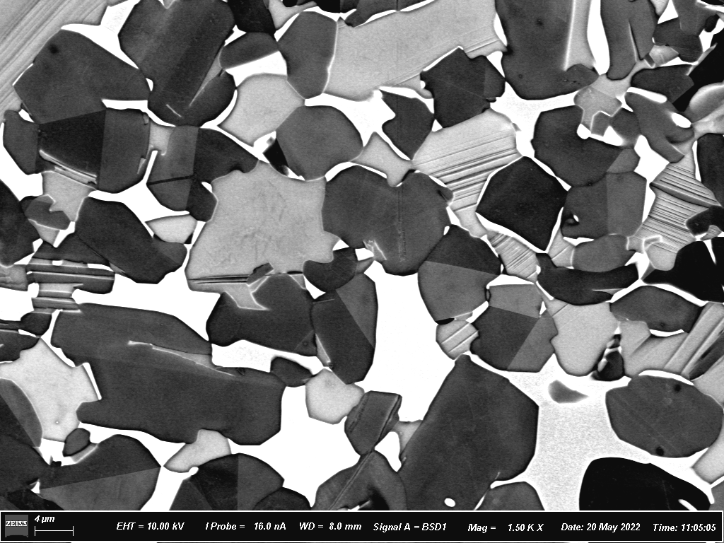
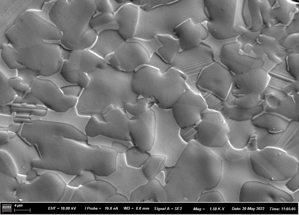
Detectors:
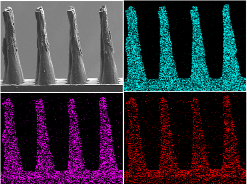
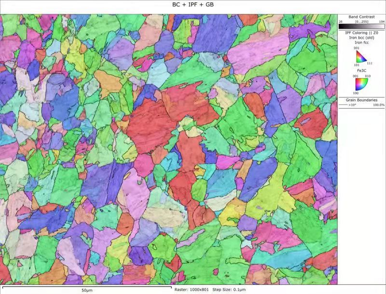
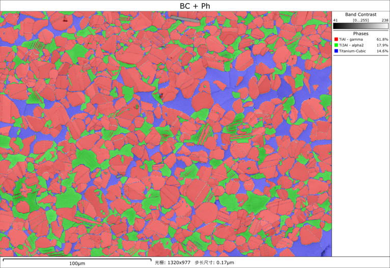
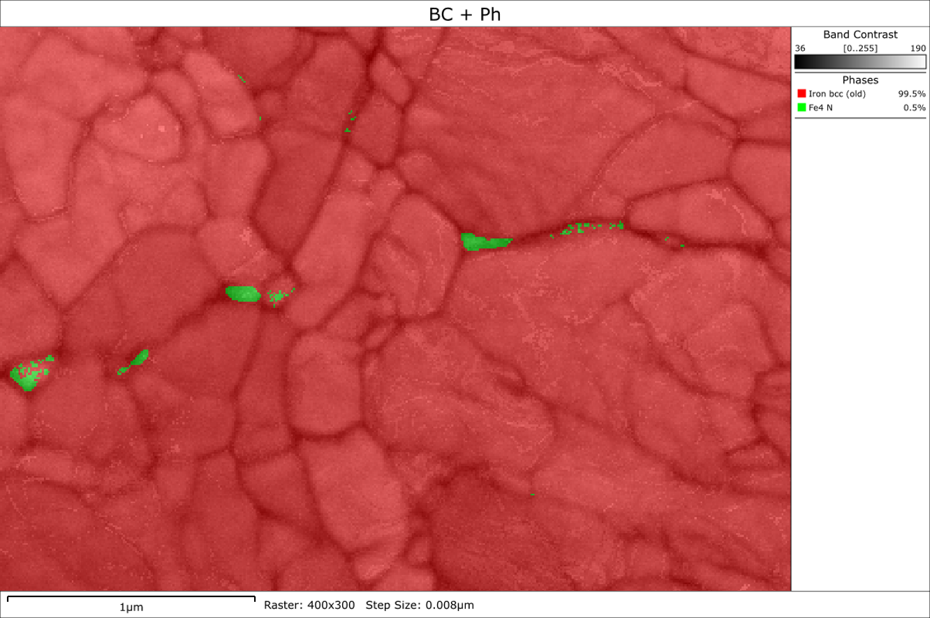
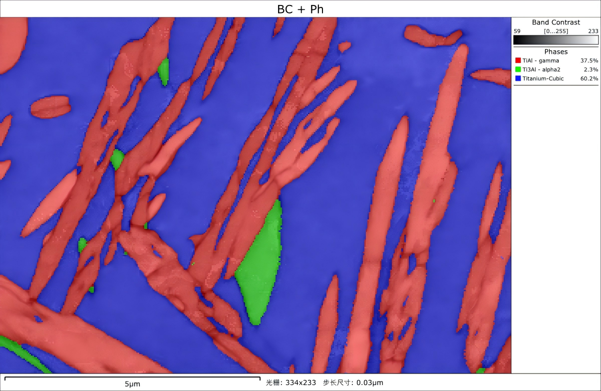
Inlens SE, SE2, ESB, BSD, VPBSD, VPSE, STEM, EDS, EBSD
Main Functions:
Contact: Jingfang Shen
Tel: 0754-88077154
Email: jingfang.shen@gtiit.edu.cn
Relevant news: Explore the Microcosm with Scanning Electron Microscope (SEM)